For this method you will need to access your WordPress site’s root folder by using FTP or File Manager app in your hosting account’s cPanel dashboard.
In most cases if you are on a shared host, then you will not see a php.ini file in your directory. If you do not see one, then create a file called php.ini and upload it in the root folder. In that file add the following code:
 # simple neural network code example on Colab
import tensorflow as tf
from tensorflow import keras
import numpy as np

model = keras.Sequential([keras.layers.Dense(units=1,input_shape=[1])])
model.compile(optimizer='sgd',loss=keras.losses.MeanSquaredError())

xs = np.array([-1.0,0.0,1.0,2.0,3.0,4.0],dtype=float)
ys = np.array([-3.0,-1.0,1.0,3.0,5.0,7.0],dtype=float)

model.fit(xs, ys, epochs=500)

print(model.predict([10.0]))
Aerosol Jet Printing (AJP) is an emerging contactless direct write approach aimed at the production of fine features on a wide range of substrates. Originally developed for the manufacture of electronic circuitry, the technology has been explored for a range of applications, including, active and passive electronic components, actuators, sensors, as well as a variety of selective chemical and biological responses. Freeform deposition, coupled with a relatively large stand-off distance, is enabling researchers to produce devices with increased geometric complexity compared to conventional manufacturing or more commonly used direct write approaches. Wide material compatibility, high resolution and independence of orientation have provided novelty in a number of applications when AJP is conducted as a digitally driven approach for integrated manufacture. This overview of the technology will summarise the underlying principles of AJP, review applications of the technology and discuss the hurdles to more widespread industry adoption. Finally, this paper will hypothesise where gains may be realised through this assistive manufacturing process.
aerosol jet vs ink jet
Dear Mr. Jiang,in my opinion, there are three major differences between the aerosol jet and ink-jet printing:1. Print resolution;2. Viscosity of ink (suspensions);3. The distance from the printhead to the substrate.1. Aerosol printing allows to achieve a higher print resolution, namely, almost 2-4 times higher than inkjet.(Typical resolution printing with a of aerosol jet is 10 microns, several studies reported print resolution of about 5 microns, while using typical ink jet printing is a minimum resolution of 20-25 microns).2. Method of aerosol jet have less strict requirements for the viscosity of ink (suspension), and therefore, a larger amount of materials (including ceramics, metals, etc.) can be printed by using an aerosol jet.(Typical range of viscosity of ink (suspension) for aerosol jet is in the range from 0.5 to 2000 cP, while the ink jet ink is used with a low viscosity, typically less than 20 cP).3. Aerosol jet has a greater opportunity to vary the distance between the print head to the substrate. Therefore, it is possible to print on non-flat (non-smooth) substrates. In of aerosol jet is possible to create 3D-contacts that inkjet is practically impossible.(A typical distance between the print head to the substrate in the aerosol jet is 1-5 mm, while the ink jet distance is fixed and must be equal, typically 1 mm)However, it is worth noting that the technology of aerosol printing is a younger technology compared to inkjet printing, the 2000s and 1950s, respectively. Consequently, the ink-jet printing more advanced technology, and you have more opportunities to find how to use inkjet printing to apply those or other structures. I also think that inkjet printing is a cheaper way of printing.
For comparison, an industrial aerosol jet printer costs about 500k USD, and the industrial inkjet printer about 200k USD, although it can be found for 50k USD (as a reference).Regarding the possibilities to form structures using ceramic materials and aerosol jet, I recommend the following article: DOI: 10.1016/j.jpowsour.2012.09.094.The last article compared the aerosol jet and ink-jet printing can be found here: DOI: 10.1021/ie503636cSee also the attached picture (Aerosol jet vs Ink Jet.gif).
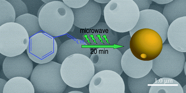
One-step facile synthesis of monoporous polymer microspheres via microwave-controlled dispersion polymerization is introduced. This template-free method employing the dispersion polymerization of styrene under microwave irradiation induces directly the formation of uniform monoporous polymer microspheres, with controllable morphologies and sizes, which can be tuned by simply adjusting parameters for the synthesis. A comparison to conventional heating indicates that microwave irradiation plays a vital role in the formation of this novel morphology.
Deep Subwavelength-Scale Light Focusing and Confinement in Nanohole-Structured Mesoscale Dielectric Spheres
One of the most captivating properties of dielectric mesoscale particles is their ability to form a sub-diffraction limited-field localization region, near their shadow surfaces. However, the transverse size of the field localization region of a dielectric mesoscale particle is usually larger than λ/3. In this present paper, for the first time, we present numerical simulations to demonstrate that the size of the electromagnetic field that forms in the localized region of the dielectric mesoscale sphere can be significantly reduced by introducing a nanohole structure at its shadow surface, which improves the spatial resolution up to λ/40 and beyond the solid immersion diffraction limit of λ/2n. The proposed nanohole-structured microparticles can be made from common natural optical materials, such as glass, and are important for advancing the particle-lens-based super-resolution technologies, including sub-diffraction imaging, interferometry, surface fabrication, enhanced Raman scattering, nanoparticles synthesis, optical tweezer, etc.
荧光纳米金刚石(Fluorescent nanodiamonds,FND)中氮空位(nitrogen-vacancy,NV)缺陷的量子自旋特性,不仅在量子计算和通信领域应用广泛,其荧光性能也十分优异,包括高量子产率,无光闪烁或光漂白,高稳定以及低毒性等。在磁场量化、温度传感和生物标记等方向上也存在着广泛的应用。与中性(NV0)中心不同,NV–中心的主要优势在于,其荧光可以通过自旋调控的方式进行选择性调节,从而在高背景环境中实现信号分离。传染病对全球健康构成了巨大挑战,而早期的诊断对于各种传染病有效的治疗和预防至关重要。目前对传染病病毒,如艾滋病病毒(HIV)或是新冠病毒(Covid-19)检测的方法较为繁琐,且需要较长时间。而与妊娠测试相似的纸基侧向流动测试(lateral flow assay, LFA)则是一种便捷的检测方法。其工作方式为将纸的一端浸入样本中,通过颜色(或荧光信号)的变化与否进行诊断。这种方法便捷且迅速,无需在实验室中处理结果。然而,当前基于纳米颗粒的生物传感器的灵敏度仍然欠缺。近日,英国伦敦大学的Benjamin S. Miller等与Rachel A. McKendry课题组合作,将荧光纳米金刚石用作体外诊断的超灵敏标签,并通过微波调节发射强度与频域分析,将信号与背景荧光信号分离,突破了灵敏度的限制。基于该技术的低成本检测试纸,对生物素-亲和素模型的检测极限达到了8.2×10⁻¹⁹摩尔。在对HIV病毒检测实验中,比传统使用金纳米颗粒的检测灵敏度提高了98000倍。此外,由于HIV病毒相对于抗原和抗体能够更早的被检测到(分别提早7天与16天),因此与现有的基于实验室的核酸检测或即时蛋白检测相比,该技术提供了更早诊断的潜力。除了HIV病毒之外,该技术还适用于SARS-CoV-2病毒,并正在进行新冠病毒的试点。该研究以题为“Spin-enhanced nanodiamond biosensing for ultrasensitive diagnostics”的论文发表在最新一期的《Nature》上。
基于纳米金刚石的侧向流动测试的检测极限第一作者Benjamin S. Miller博士表示,基于纸的测向流动测试避免了繁琐的实验室分析,显著提升了测试便捷性与及时性,同时大大降低了成本,这使得它们在资源贫乏地区特别适用。另一位通讯作者Rachel A. McKendry表示,该技术非常灵活,可以轻松适应其他疾病和生物标记物类型。当下研究团队正在进行该技术在新冠病毒检测方面的研究。Rachel A. McKendry相信,这种变革性的新技术将使患者受益,并保护人们免受传染病的侵害。


